
Moore Law and AI Infra Investment Framework

“For modern AI workloads, data movement is as critical as computation itself” -Tingbo He, Huawei
Excluding non-market factors and colors, Huawei's τ law can be understood as the same thing as Lao Huang's extreme co-design: in the context of the exponential explosion of AI's computing demand, the cost increase per unit of computing power has been limited through scaling up transistor density. In the future, system-level improvements such as advanced packaging, PCB, internal and external interconnection, and even power supply upgrades will be needed to significantly increase efficiency and reduce costs.
In fact, NVIDIA is no longer just designing chips. It has already covered the connection methods of various chips, the design of power supplies and liquid cooling inside and outside the cabinet and even the entire data center to improve computing efficiency.
Huawei talked about this matter in a more exciting way, explaining that the essence of what shrinkage technology does is to increase the signal transmission speed of 0 and 1, and the signal transmission speed can be bypassed/dilute the stuck shrinkage technology through advanced packaging/optical interconnection, etc.
The two companies said the same thing in very different ways. Expressed in vague numbers: Assume that Moore’s Law/microscale technology is responsible for ~90% of the credit for promoting the digitization of the world and the reduction of computing costs; in the context of AI, Moore’s Law/microscale technology may only account for ~50% of the credit
Translated into investment terms: Under the trillion-level AI capex, many core links other than computing power, especially links, will definitely increase their share of AI capex, and will generate many structural opportunities.
There is a good summary formula in the τ law article: signal transmission efficiency is not only achieved through transistor technology, but also through various other improvements such as circuit circuits (such as hybrid bonding), chip chips, and system systems (such as NPO and UB transmission protocols).

Source: A Time Scaling Theory for Multi-Layer Electronic Systems
From an investment perspective, we have a similar framework, which is to find the so-called bottleneck links that can best reduce the "τ" value in the overall AI data center construction, players who promote technological progress in these links, and then select links with relatively good competition and low risk of technology substitution.
From the distance of signal transmission, it can be roughly divided into four links, as well as the corresponding "τ" law framework: advanced packaging, PCB, Scale up & Scale out

Each link is undergoing very big changes on both the supply and demand sides. Let’s just talk about some very interesting directions we have seen. It does not represent any investment views.
Advanced Packaging: The “TSMC Moment” for the Packaging Industry?
Advanced packaging, especially hybrid bonding, is the most mentioned technology in the τ law. The current mainstream advanced packaging is CoWoS (2.5D packaging). The computing chip and HBM are placed on the silicon interposer, which is like setting up a highway on the ground. The signal must travel horizontally to connect the two ends; while hybrid bonding is more like building directly on the spot, connecting die to die in the vertical direction through Cu-Cu direct copper-copper bonding. The signal goes straight up and down like an elevator, with almost no need to "drive". The distance comparison is subversive: CoWoS is 1-10 mm horizontally, and hybrid bonding is only 0.01-0.1 mm vertically, which is hundreds of times shorter; the density of linked lines per square millimeter has also increased from ~1000 levels to 10,000/100,000 levels
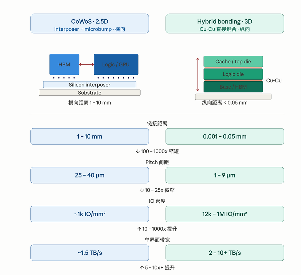
The alignment accuracy required for hybrid bonding equipment has entered the nanometer level (sub-100nm), which is the same order of magnitude as the alignment accuracy of semiconductor front-end lithography, and the required clean room level is also close to fab. What is interesting is not only this technical route and this equipment, but the changes it represents in the entire advanced packaging industry. Just like semiconductor foundries, it is a relatively fiercely competitive business in mature processes, but the competitive landscape in advanced processes is clearly differentiated. Packaging factories are also showing signs of this: the packaging task of a chip has gone from requiring only one packaging equipment to requiring an expensive production line with more than 20 machines, and knowledge of every link.
PCB: Another sprint to the physical limits of upstream materials
A recent research report from Morgan Stanley was very popular, which mentioned that the proportion of PCB in Vera Rubin cabinet UE has increased second only to storage. There is an underlying physical knowledge that needs to be understood. The signals required by AI can be "parallel wired" within ~20mm (that is, inside the GPU package and on the substrate). However, outside this range, that is, when the signal is transmitted to the PCB, the signal needs to be "serial wired."

What this brings is an exponential increase in the number of copper wires on the PCB * the rate requirements that each wire can bear, which corresponds to the number of layers and materials of a single PCB in the PCB industry. The logic behind the improvement of PCB UE is that the demand for signal transmission is faster than the demand for computing power.
There are also many interesting links and companies in this field. The most touching one is the materials link. We see that driven by AI needs, humans are once again sprinting towards the physical limits of various basic materials.
For example, copper foil, because the signal travels on the surface of the copper foil, the rougher it is, the more roads it travels up and down, and the smoother it is, the fewer roads it travels. So now everyone needs to make the smoothness of copper foil less than 0.5 microns... Yes, it is another nano-level link.

Source: Mitsui Kinzoku
Scale up / scale out: "light advances and copper retreats"
Now we have entered the section that everyone immediately thinks of when mentioning AI links, scale up and scale out.
This part of the trend cannot escape the laws of physics. As the speed increases, the distance that can be efficiently transmitted using copper as a medium is getting shorter and shorter. The signal has to change to a medium, from copper to light.

Source: Corning
But the structural investment research confirmation in this part is a headache: optical modules/LPO/NPO/CPO/OCS and other technical routes, each technical route has different solutions (such as silicon photonics vs EML vs TFLN for optical modules, MEMS vs silicon photonic waveguide for OCS...). The key point is to find some links where the risk of technical iteration is small and can exist for a long time.
Scale across / DCI: High bandwidth demands spill over a single data center
Based on the current data center construction plan, the average scale-across bandwidth per GPU is still very low. However, this part of the bandwidth, whether due to the training needs of the 100,000-card cluster or the demand for inference data centers closer to customers brought by agent workflow, is likely to increase rapidly in the future.
You can refer to the recently published article: (Insert previously published DCI article here)

Write at the end:
AI link is indeed a relatively complex and rapidly changing industry, and the boundaries of each link are beginning to blur. Players from all parties compete across borders, and each link replaces each other. Without AI, it is no longer possible to invest in the AI field. Doing investment research in this industry may be the best use case to re-create the investment research workflow based on AI.



Comments